
Interacting with Devices via PSS Registers
18 Apr 2023
We’ve been looking at properly modeling the types of behaviors that we want to exercise on our DMA IP for the last few posts. Of course, until we can actually start programming the DMA registers, all of our modeling won’t actually do anything.
PSS provides two primary ways to connect the model of test behavior we want to exercise to the device on which we will exercise that behavior:
- Calling functions that are implemented in the target environment
- Using PSS features to read/write registers and memory
Both of these approaches have benefits and drawbacks. If functions already exist to program IP registers, leveraging these from PSS helps to get tests up and running more quickly. However, functions are typically only implemented in a single language. Greater portability is achieved by directly describing the interactions between PSS model and device registers in PSS.
This post will look at describing the register interface using the PSS register model.
Registers in Different Contexts
Looking across the various contexts in which registers appear, it quickly becomes clear that the critical capabilities are quite different.
- Within the RTL implementation of an IP, registers communicate control values set by firmware to the implementing logic and feed back status data from hardware to firmware. In addition, some degree of change event may be useful (eg register written). In other words, data storage and the structure of that data are the key care-abouts here.
- In a UVM block-level verification environment, there are a significant number of overlapping requirements. A UVM register model captures the structure of data within registers (eg named fields), and layout of registers within memory. A UVM register model enables a shadow copy of register contents to be maintained for debug and analysis purposes. Since access to registers is typically via a memory-mapped address space, the register model supports mapping between high-level changes to register values and writes to the addresses of those modified registers. All in all, the UVM register model may be the most complex that we work with.
- At system level, we interact with the registers in our IP blocks and subsystems using firmware. When we’re writing this firmware by hand, it’s typical to have a set of C ‘#define’ macros that help to calculate the address of registers, and that extract and set the value of register fields. At this level, there’s little to no value in caching a copy of the last known value of a device register.
Because PSS has a system-level focus, it’s probably no surprise that it focuses on the key capabilities required at system level: being able to efficiently model how registers fit into the address space space of a device, and efficiently read and write them. Unlike the UVM register model, the PSS register model doesn’t maintain a copy of the data stored in registers.
The PSS Register Model
The PSS register model focuses on capturing the field layout of each register, the layout of device registers in the memory map, and on providing efficient mechanisms for reading and writing to the device registers.
The key elements to be aware of are:
- Register group component that collects registers and sub-groups of registers together
- Register component that describes a single register – often in-line
- Register definition struct that describes the fields of a register
Both the register group and register components are pre-defined components defined by the PSS Core Library. While they are not built-in constructs in the language, they are special types that tools are expected to implement specially.
Register Group
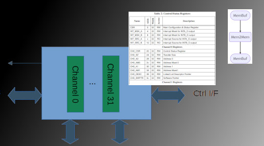
We define a register group to contain the top-level registers and register groups of a device (eg our DMA engine). Or, any time we collections of registers that we want to use mulitple times.

Let’s look at the first part of the DMA Engine registers (shown above). We have some control registers that are common across all of the DMA channels. Then, groups of registers that are replicated for each channel.
We will create a register group for the full set of DMA engine registers and a register group for the per-channel registers. The full DMA engine register group will contain both the individual registers and an array of the per-channel register groups.
pure component WbDmaChannelRegs : reg_group_c {
    // ...
}

pure component WbDmaRegs : reg_group_c {
    // ...

    WbDmaChannelRegs        channels[31];
}
Register Definition Struct and Component
Each register is composed of some number of fields. When these fields have
special meaning, we define a packed struct to capture the field layout.
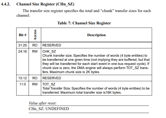
The image above shows the layout of the size register within the block of per-channel registers. We declare the struct below to capture the layout of the fields in the register. Note that the start of the first field in the struct corresponds to the lowest bit in the register.
struct WbDmaChannelSz : packed_s<> {
    bit[12]           TOT_SZ;
    bit[4]            RESERVED_1;
    bit[9]            CHK_SZ;
    bit[7]            RESERVED_2;
}
The struct shown above just defines the layout of data within a register.
pure component WbDmaChannelRegs : reg_group_c {
    reg_c<WbDmaChannelCSR>         CSR;
    reg_c<WbDmaChannelSZ>          SZ;
    reg_c<bit[32]>                 SrcAddr;
    reg_c<bit[32]>                 SrcAddrMask;
    reg_c<bit[32]>                 DstAddr;
    reg_c<bit[32]>                 DstAddrMask;
    reg_c<bit[32]>                 LinkListPtr;
    reg_c<bit[32]>                 SwPtr;
}
When declaring a register within a register group, we add a field
of type reg_c that is parameterized with the data type
that describes the register. This core data type could be a packed
struct as is shown above. It could also be an integer in cases where
giving names to all the fields isn’t so important.
For example, we use packed structs to define the layout of the CSR and SZ fields. Address and address-mask fields are defined using plain integer data types.
From this point on, we simply build up. We define a register struct
for any register whose field layout we care about. We add a
type-parameterized reg_c field for each register to its containing
register group, and fields of reg_group_c type for instances
of register groups.
pure component WbDmaRegs : reg_group_c {
    reg_c<WbDmaCSR>         CSR;
    reg_c<bit[32]>          INT_MSK_A;
    reg_c<bit[32]>          INT_MSK_B;
    reg_c<bit[32]>          INT_SRC_A;
    reg_c<bit[32]>          INT_SRC_B;

    WbDmaChannelRegs        channels[31];
}
For the DMA engine, this process results in a top-level register block for the IP such as the one shown above. In this case, we have a few individual registers and an array of channel register groups.
The PSS Register Model in the Real World
In the prior sections, we manually created a PSS register model.
In practice this is quite rare because, in a production environment,
all of the various register descriptions
(RTL, UVM, firmware, documentation, etc)
are derived automatically from a single description. That
central description might be captured in a spreadsheet or
CSV file, IP-XACT document [3], or a SystemRDL description [1].
Personally, I’m very interested in SystemRDL. My feeling is that it’s easier to create and modify than IP-XACT, and I just learned about an open source toolchain named PeakRDL that can be used to derive various outputs from it.
As you begin to look at applying PSS in your environment, it’s a good idea to understand what single representation your organization uses for register information, and what facilities exist for adding new automatically-derived output formats.
Instantiating and Connecting the Register Model
Our PSS register model is simply a mechanism for associating the addresses and bit patterns of memory-mapped registers with symbolic representations. Consequently, we need to connect our register model to an address space before we can actually use it for reading and writing registers.
Connecting to Register Space
Registers are always mapped at some location within the address space. In order to determine the correct address to use when accessing a register, we need to know where its containing register model is located in memory.
component pss_top {
    transparent_addr_space_c<>               aspace;
    addr_handle_t                            mmio_h;

    WbDma                                    dma;

    exec init_down {
        transparent_addr_region_s<>          region;

        region.addr = 0x8000_0000;
        region.size = 0x1000_0000;
        aspace.add_region(region);

        region.addr = 0x0000_0000;
        region.size = 0x1000_0000;
        aspace.add_region(region);

        region.addr = 0x1000_0000;
        region.size = 0x1000_0000;
        mmio_h = aspace.add_nonallocatable_region(region);

    }
}
The code above shows defining a region within the memory
map that is defined as non-allocatable. In other words,
we cannot use addr_claim_s fields within actions to
claim memory from this region. Note that
add_nonallocatable_region returns an address handle that we save.
We will use this handle to specify where the register block
is located.
Connecting
In this little example, the register model that we’re focusing on is the one and only register model. This is not the case most of the time. It’s much more frequently the case that the register model for our IP is just one part of much larger system-level register model.
Generally speaking, PSS provides two different strategies for associating a component with the register model it should use, and associating the register model with the base address it must use:
- We can create a large register model that has a base address and distribute references to register sub-models to components
- We can create a register model per consumer component and calculate a base address to associate with each.
Large Register Model ; Distribute Refs
In this scheme, our DMA component has a reference to the register model, not an instance:
component WbDma {

    pool MemBuf     mem_buf_p;
    bind mem_buf_p  *;

    pool [16] Channel    channels_p;
    bind channels_p *;

    // Handle to the register model
    ref WbDmaRegs           regs;

    // ...
}
The code that uses the register model doesn’t care whether it is using a reference or an instance of a register model. Either way, registers get written and read.
The register for all instances of our DMA engine are included in the top-level register model, as shown below.
pure component SysRegModel : reg_group_c<> {
    // ...
    WbDmaRegs           dma0;
    // ...
}
Finally, our system-level register model is instanced at the top level of the component tree.
component pss_top {
    transparent_addr_space_c<>               aspace;
    addr_handle_t                            mmio_h;

    SysRegModel                              regs;

    WbDma                                    dma0;

    exec init_down {
        transparent_addr_region_s<>          region;

        // ...
        region.addr = 0x1000_0000;
        region.size = 0x1000_0000;
        mmio_h = aspace.add_nonallocatable_region(region);

        regs.set_handle(mmio_h);

        dma.regs = regs.dma0;
    }
}
A few things are going on here:
- After obtaining a handle to the root of the memory-mapped I/O
space, we configure this as the base address of the system
register map by calling the
set_handlefunction on the system register model. - Next, we hook set the register-model reference field in the dma0 component instance to point to its instance of the register in the system register model.
And, with that we’re done. The advantages of this approach are that we’re only concerned with the base address of the full register space and it might be easier to construct this ‘super’ register model using automation tools. We also have the option to directly reach down through the register model to access registers. The biggest downside is a loss of some degree of modularity.
Individual Register Models ; Distribute Base Addresses
This approach is nearly mirror image of the previous approach. In this approach, each component with registers “owns” its register block and we distribute base-address handles.
So, here’s the DMA component:
component WbDma {

    pool MemBuf     mem_buf_p;
    bind mem_buf_p  *;

    pool [16] Channel    channels_p;
    bind channels_p *;

    // DMA register model
    WbDmaRegs           regs;

    // ...
}
Note that we have full register model instance here, instead of just a reference.
component pss_top {
    transparent_addr_space_c<>               aspace;
    addr_handle_t                            mmio_h;

    WbDma                                    dma;

    exec init_down {
        transparent_addr_region_s<>          region;

        // ...

        region.addr = 0x1000_0000;
        region.size = 0x1000_0000;
        mmio_h = aspace.add_nonallocatable_region(region);

        dma.regs.set_handle(make_handle_from_handle(mmio_h, 0x1000));
    }
}
At the top level, things are a bit different as well. There is not unified top-level register model. Instead of setting the DMA register-model handle within the DMA component, we set the base address handle on the register-model instance within the DMA component. Note that we need to compute the proper offset to create the correct address handle for the DMA registers.
Using the Register Model
Now that we have our register model integrated and connected, we can write PSS test realization code to program a DMA channel to perform a transfer.
action Mem2Mem {
    // ...

    exec body {
        // Setup the transfer size
        WbDmaChannelSZ sz;
        sz.CHK_SZ = 16;
        sz.TOT_SZ = dst_o.size / 4; // We always work in words
        regs.SZ.write(sz);

        // Configure source and destination addresses
        regs.INT_SRC_A.write_val(addr_value(src_i.addr_h));
        regs.INT_DST_A.write_val(addr_value(dst_o.addr_h));

        // Enable the channel
        WbDmaChannelCSR csr = regs.CSR.read();
        csr.CH_EN = 1;
        regs.CSR.write(csr);

        // Wait for the transfer to complete
        repeat {
            csr = regs.CSR.read();
            // ...
        } while (csr.DONE == 0);
    }
}
First, we’ll want to configure a couple of details about the size of the transfer. For this, we use the WbDmaChannelSZ packed struct to properly format data to write to the register.
Next, we’ll setup the source and destination addresses. For these, we will
use the write_val function to just write the address value to the register.
We need to enable the channel before the transfer will start. To do this,
we want to modify a bit within the configuration and status register while
leaving the other fields as-is. To do this, we can read the value of the
CSR into a register struct, set the CH_EN bit, then write it back
to the register.
At this point, the DMA engine will begin transferring memory. Finally, we
need to wait until the channel’s DONE bit is set. This signals that the
transfer is complete. Here, again, we use the register struct to make it
easy to extract the bits that we care about.
This code is concise and easy to write – generally much more so than the equivalent hand-coded bare-metal C code. The great thing, of course, is that the resulting implementation is just as efficient as if it were hand-coded in C.
Conclusion and Next Steps
We have now worked through all the key topics in exercising the memory to memory copy functionality of our DMA engine. We’ve looked at:
- Buffers to represent data transfer between sequential actions
- Memory management to remove complexity from our tests
- Resource management to ensure concurrent test behavior doesn’t collide over resource usage like DMA channels
- And finally, using the PSS register model to capture the layout of registers and register blocks, and access device registers.
But, if you remember, there is one other key part of the DMA engine’s functionality: supporting DMA transfer for peripheral devices without their own internal DMA engines. Modeling this type of behavior brings unique challenges. Especially so when we want to be able to exercise that behavior with multiple different devices at the system. In the next post, we’ll look at approaches for modeling this with PSS.
Resources
- [1] SystemRDL 2.0 LRM
- [2] PeakRDL
- [3] IP-XACT
- [4] DMA Example (Viewing)
- [5] DMA Example (Raw Text)